Implementation of a Programmable System-On-Chip (PSoC) on a FPGA
In this project pseudo-randomly numbers are generated on a module of FPGA and sorted using different algorithms which are mounted on an 32-bit Nios II embedded soft-processor. Then these numbers are sorted in ascending in the Nios II soft-processor (implemented on other module of FPGA) and shown in the terminal of Nios II SDK.
These modules were designed using the hardware description language VHDL on Quartus II 13.0 and implemented in the Cyclone III device family. To the hierarchical design of this system we will use QSYS and Nios II SDK tools from Quartus II to create the processor and the software respectively.
The next image show the schematic of al the system implemented on the FPGA, each module is implemented in VHDL except processor wich is implemented using Qsys.
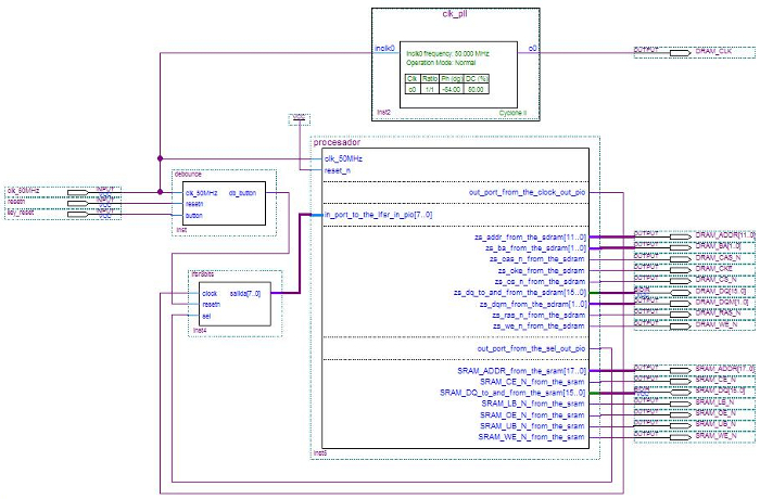
Figure 1: Schematic of the system implemented on the FPGA
Principal components are described in the next part:
- debounce: Implements a circuit for eliminating the rebounds caused by pressing a button ('key_reset' signal). Each time the button is pressed, the signal passes 'key_reset' '0' but rebounds, and release the button, the signal passes 'key_reset' '1' but rebounds. 'db_button' signal produces a pulse (active low) free rebounds effect of pressed and released the button.
- lfsr8bits: This module implements two circuits. The first of these is an 8-bit counter upwards. The second is a pseudo random generator using 8-bit LFSR (Linear Feedback Shift Register) technique. Generating account settings (pseudo random or sequential upward) occur with the rising edge of the clock signal.
These pseudo random numbers are generated using an initial value of "00000000" and using the polynomial x^8 + x^4 + x^3 + x^2 + 1, which produces 255 different output values to random.
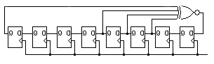
Figure 2: Schematic Moore Machine
- procesador: This block is generated by the SoPC Builder tool. Having an input port of 8 bits called 'lfsr_in_pio' (read the value generated by the 'lfsr8bits' block) and two output ports of 1 bit. A port is called 'clock_out_pio' (block clock signal 'lfsr8bits') and the other (signal "'sel'" lfsr8bits block) is called 'sel_out_pio' where 'clock_out_pio' and 'sel_out_pio' generated in a program in ANSI C. The block processor has interfaces to SDRAM Memory and SRAM.
- clk_pll: This block is a PLL used to generate the clock signal to be applied to the card memory SDRAM Altera DE0 where the project is implemented.
Algorithm
For the realization of our computer data in ANSI C program has been used Quicksort sorting algorithm, which consists of choosing a pivot and then order numbers less than the pivot to the left of the pivot, and numbers greater than the pivot right pivot. This pivot choose it as the data that occupies one of the central positions of the array A [256] (here under [256] saved sludge find the values of our SRAM to be ordered). After having ordered the lower numbers pivot left and right numbers rights proceed to elect our new pivot and proceed to make the right ordering of the largest numbers and left lower numbers again.
The next image shows the result of sorter algorithm:
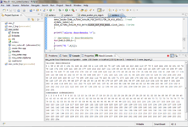
Figure 3: Result of sorter algorithm implemented on Nios II processor