CMOS design of FPGA's Programmable Interconnect Points
Field Programmable Gate Arrays (FPGA) are very interesting integrated circuits. The possibility of completing different tasks by just reprogramming the FPGA made us think at first view it was a kind of microcontroller. We were far from the reality. FPGAs are reprogrammable logic/memory circuits and can be faster than any microcontroller. The main difference is that a microcontroller has a program written in memory, and a FPGA only has programmed connections/cells, so the data follows a continuous way through programmed logic and memory cells, instead of being processed by only one ALU.
Programmable Interconnect Points are vital to any FPGA, they allow us to link the output of a cell, or an input pad of the FPGA to any other cell/Pad in the circuit by making a “path” for the data through the FPGA. Every way is fixed during the programming by connecting metal lines with PIPs. These PIPs, well named, are programmable to permit us to build any path we want.
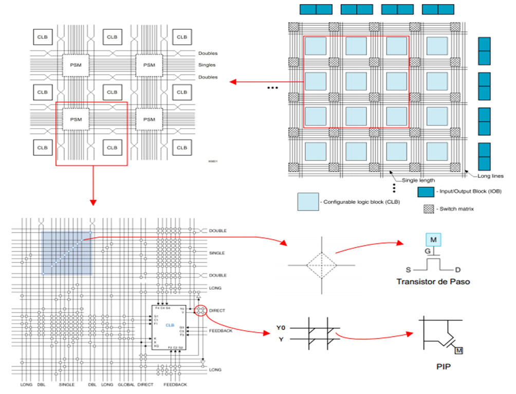
Figure 1: FPGA's Programmable Interconnect Points
Global View of a PIP array
In the example below (Drawing 1), we have drawn a 4x4 PIP array . The goal is to link a column with a line by configuring the PIP at the intersection between them. For example we have configured the PIP at the intersection of column 2 and Line 3 to link them, the other are left unconnected. Then we put a signal on Column 2, and see its path on the schema.
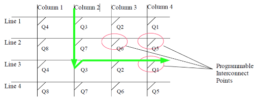
Figure 2: Example of a 4x4 PIP array
The problem that comes next is: How do I configure all this mess? The solution implying the minimal number of Inputs is to use edge-triggered DRegs to keep the state of a PIP. Then we only have to link them serially by connecting Q Output to next latch's Data Input.
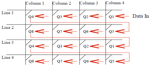
Figure 3: Propagation of the configuration data
On a falling edge of the clock, the DReg will memorize the value it has on the data input, and put it on the output after a few picoseconds. This way we can program the entire DReg chain by putting their states successively on the main Data Input. The first value will configure the state of the last DReg, and the last value will configure the first Latch.
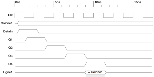
Figure 4: Timing Diagram of the propagation through the DRegs
Logic View of a Simple Programmable Interconnect Point
The first step is to design one PIP. A PIP is composed of an edge-triggered DReg and a set of 2 transistors used to make the connections. The edge-triggered DReg uses 2 memory cells having only a few differences between them, the fastest way to design the Latch is to design a memory cell, duplicate it and adapt the cells to function correctly.
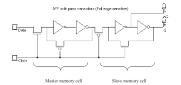
Figure 5: Logic View of a DReg
The only difference between the 2 memory cells is that the 2 MOS controlled by the clock are inverted in the slave memory cell compared to the master memory cell. The two transistors used to make connections are a P-MOS and a N-MOS. The N-MOS receives a not Q state and is used to improve performances compared to a unique transistor.
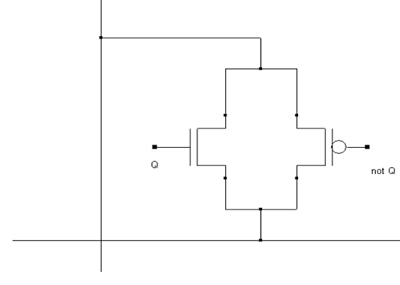
Figure 6: Logic View of a DReg
Those Q and not Q states are kept by the Dreg and accessible as outputs.
Programmable Interconnection Points Array
The goal of this step is to link PIPs to make it possible to configure all the Dregs with only 2 wires. To reach this goal we have linked the Q output of a Dreg to next Dreg's Data Input, and we have placed a Clock Line providing the clock signal everywhere in the matrix.
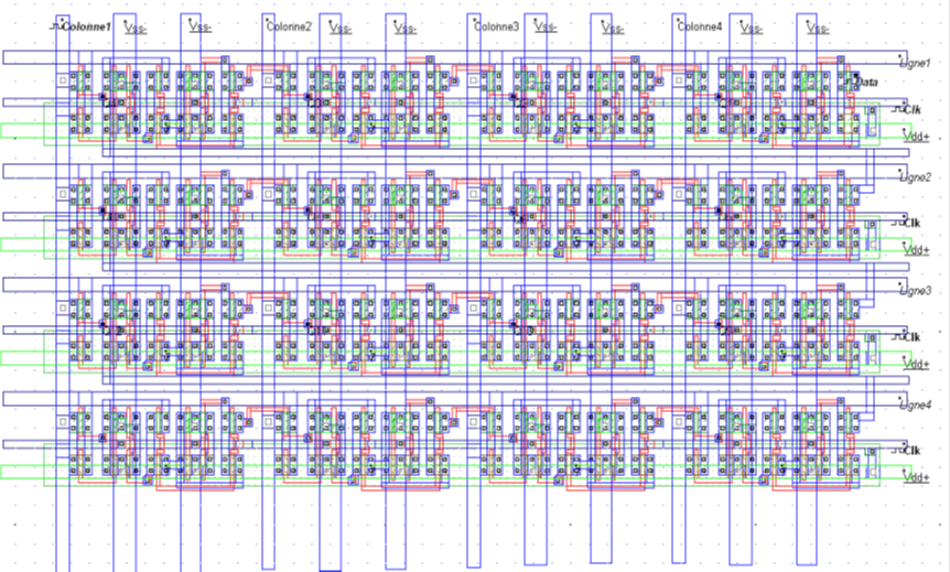
Figure 7: Global view of the PIP array
Existing proposals
The arrangement of previous PIPs has been designed to connect a line and a column, but we can not cut the lines or columns. The possibility of cutting between lines and columns would avoid a loss of surface caused by a large number of lines and columns. This type of PIP is made up of 6 programmable switches, that is to say 6 DRegs and is called the Matrix of Switching (Switch Matrix). In the figure shown below, it is observed how a switching matrix is part of an FPGA.
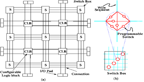
Figure 8: Switching matrix as part of an FPGA
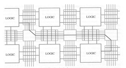
Figure 9: Switching matrix as part of an FPGA
Design principles
To design the PIP circuit, the 0.25 micron (λ = 0.125 μm) technology with a voltage of 2.5 Volts has been used. In addition a consideration that we must have is that our DReg will be activated by falling edge.
Design at the level of functional blocks
The Figure 10 shows the implemented design at the level of functional blocks uisng the logical editor and simulator Dsch 3.5. The output of each latch is connected to the input of the next latch, in other words, this design has a cascade connection, and all latches have a common clock signal.
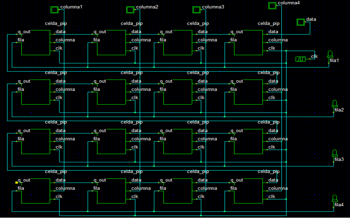
Figure 10: Design at the level of functional blocks
The design of a latch is showed in the Figure 11 and is based on the design presented in the Figure 5.
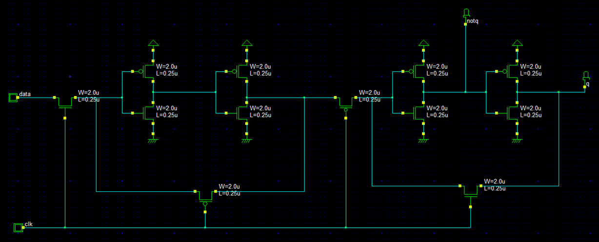
Figure 11: Design at the level of electronic circuits
The latch created above is represented by the DRed in the Figure 12. So, the 'q' and 'not q' outputs control two transistors in order to connect and disconnect the row and column. When data is 1 in the input and at falling edge of clock, then "q" takes the value of 1 and both transistors are actrivated, so and the column and row are connected. On the other hand, when data is 0 in the input and at falling edge of clock, then "q" takes the value of 0 and both transistors are desactrivated, so and the column and row are disconnected.
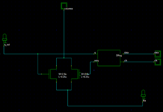
Figure 12: Design at the level of electronic circuits
At level of geometric design (Layout)
Then, the Verilog file is exported to Microwind. The results in Microwind and the geometric design level for different configurations of the latches is showed in the next Figures.
1x1 matrix
The geometric design level of one latch is showed in the Figure 13.
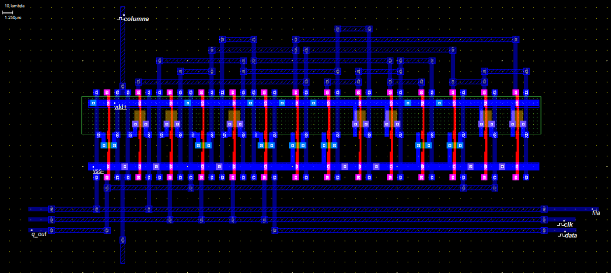
Figure 13: At the level of geometric design
The simulation of the design described above is showed in the Figure 14, and puts in evidence that when data is 1 in the input and at falling edge of clock, then "q" takes the value of 1 and both transistors are actrivated, so and the column and row are connected. On the other hand, when data is 0 in the input and at falling edge of clock, then "q" takes the value of 0 and both transistors are desactrivated, so and the column and row are disconnected.
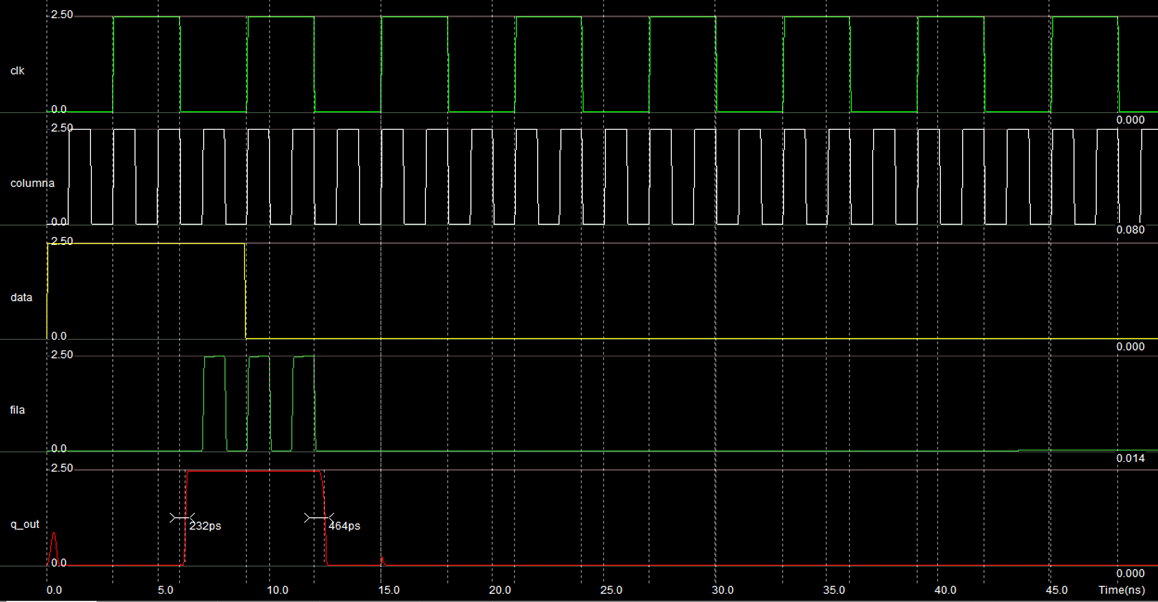
Figure 14: At the level of geometric design
2x2 matrix
Now, the design of a simple latch is expanded to 4 latches configured in a 2x2 matrix is showed in the Figure 15.
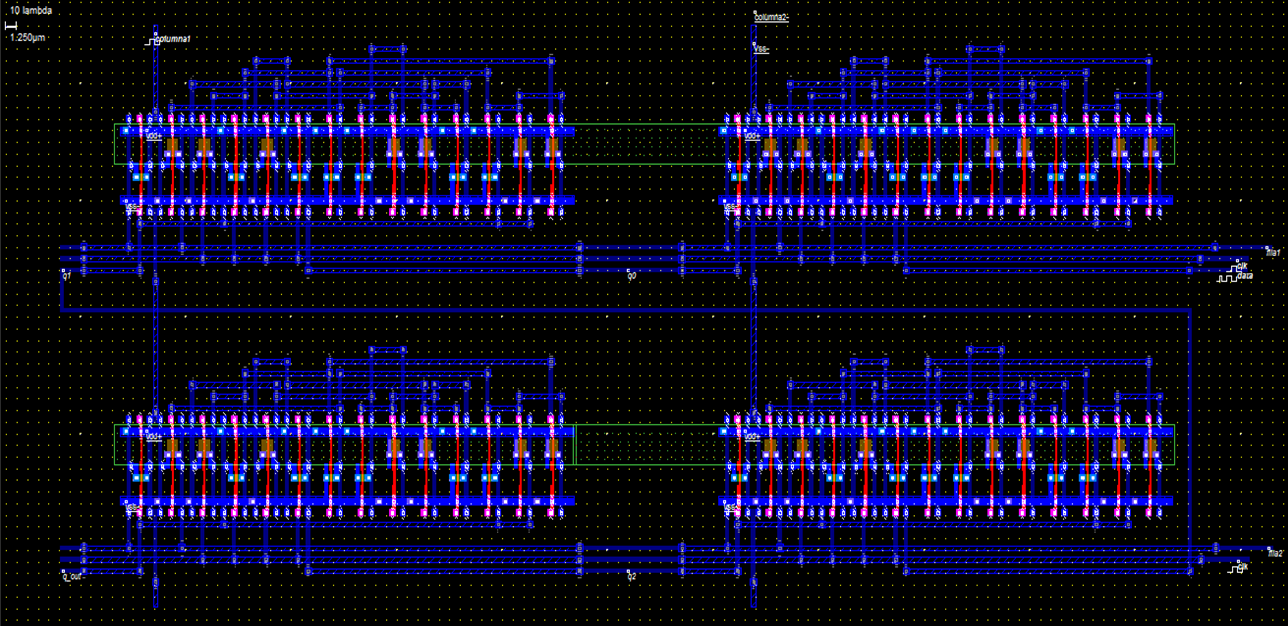
Figure 15: At the level of geometric design
Then, the simulation of the design descibed above is performed. The results verifies the correct use of the data signal to control the connection of rows with colums. For example, row 1 and column 1 are connected when data is 1 in the input q0 of the 1st latch at falling edge of clock. Also, row 2 and column 1 are connected when data is 1 in the input q2 of the 3rd latch at falling edge of clock.
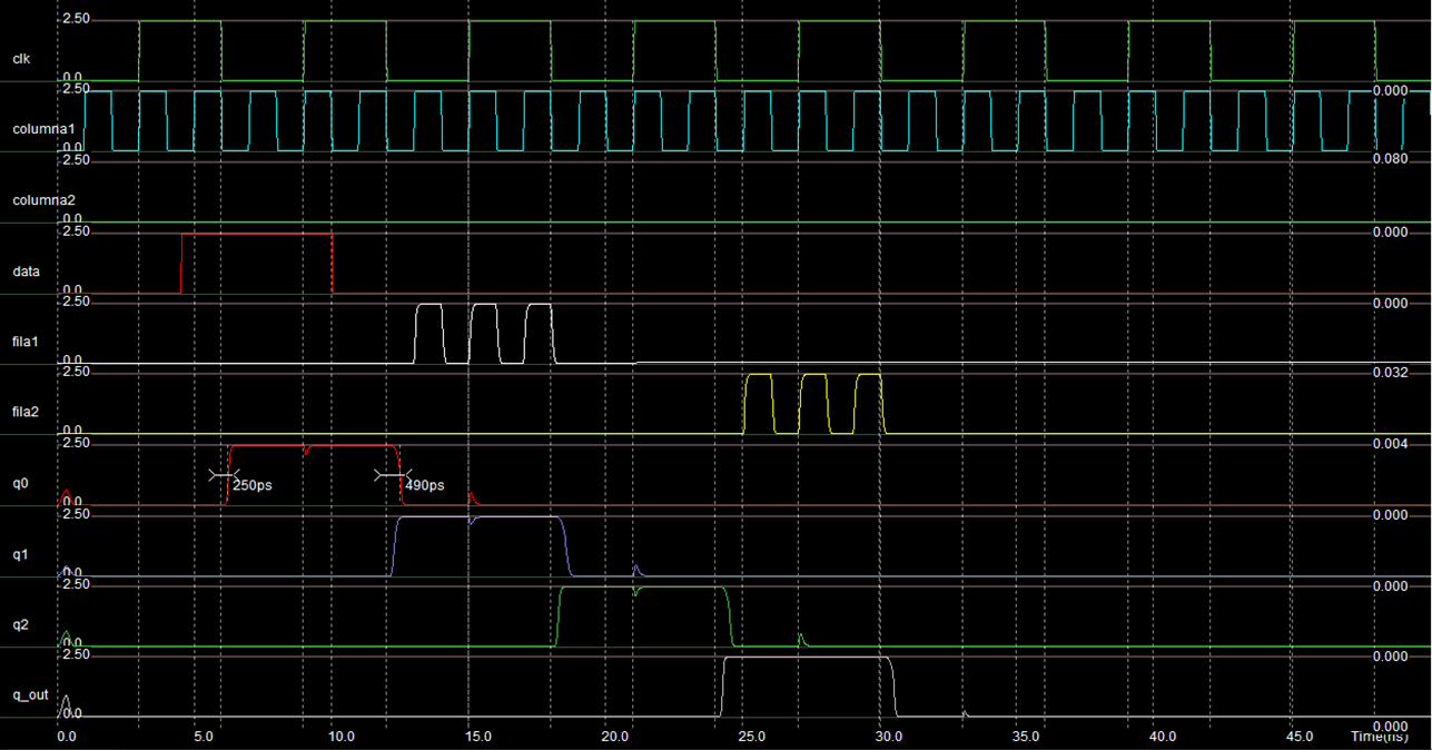
Figure 16: At the level of geometric design
4x4 matrix
The design of a simple latch is expanded to 16 latches configured in a 4x4 matrix is showed in the Figure 17.
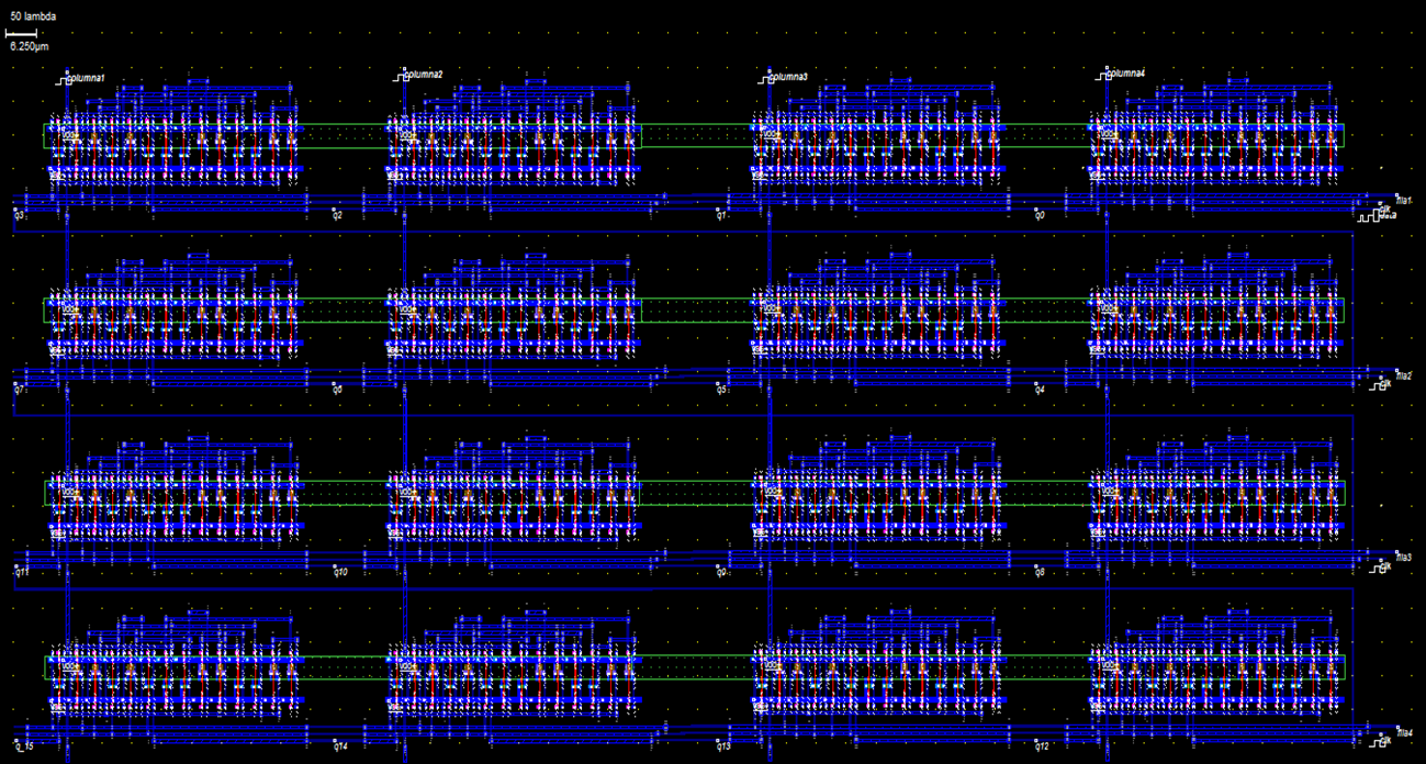
Figure 17: At the level of geometric design
The simulation of the design descibed above is showed in the Figure 18. The results verifies the correct use of the data signal to control the connection of rows with colums. For example, row 1 and column 1 are connected when data is 1 in the input q2 of the 4th latch at falling edge of clock. Also, row 3 and column 1 are connected when data is 1 in the input q10 of the 10th latch at falling edge of clock.
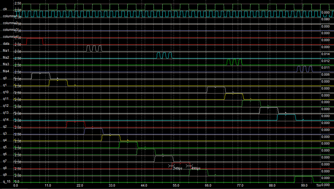
Figure 18: At the level of geometric design
From the previous simulation we also observed that:
t_(p,máx) = (249+490)/2 ps = 369.5 ps
f_máx=1/t_(p,máx) = 1/(369.5∗(10)^(−12) ) = 2.71 GHz
Also, it has a power consumption of 0.264 mW at a temperature of 27° C.
Remarks
For the design of the 4x4 PIP circuit, the software tool EDA for the design of integrated circuits Microwind 3.5 and the logical editor and simulator Dsch 3.5 have been used. Both tools have been obtained from the Microwind page (http://www.microwind.net).
As it is known, the main use of PIPs is in the FPGAs, at the same time there are two large producers of FPGAs and which are Xilinx and Altera, the same ones that have different models of FPGAs for the applications to be made.
With the advancement of technology and with the miniaturization of integrated circuits, there will be an increasing density of PIPs within an FPGA, which will make it possible to produce more efficient FPGAs, since an increase in PIPs means more of roads for the interconnection between CLB's.