Control of an analog camera with a FPGA using the parallel peripheral
This project presents the transmission of the image by SPI from the FPGA to the PIC32. This transmission is done by extracting the data from the camera through the ADV7180 codec and the image is displayed on the PC using the Matlab software tool. In the FPGA a synchronous design will be implemented and it consists of the following states: detection of image start, image recording in the SRAM, reading of the SRAM by SPI, writing of the SRAM by SPI. Of the previously mentioned states, the 'reading and writing of the SRAM by SPI' is done in order that the master (in this case the pic32) make use of the memory data and thus execute the compression algorithm implemented in the PIC32.
Taking the images with the camera, recording in the SRAM and reading / writing of the SRAM by SPI will be done using the basic scheme shown in Figure 1.
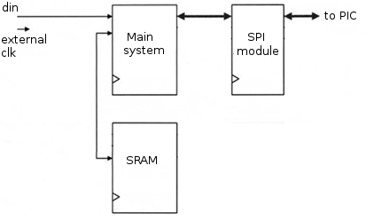
Figure 1: Basic scheme of the system
The modules used (SRAM and SPI) are administered by the Main System in the FPGA, which is also a slave of the PIC32 and is used to read and write data in the SRAM. The design will be synchronous and the external clock used will be generated by the codec ADV7180 and which is 27 MHz, in addition to Figure 1 it should be noted that the din signal corresponds to the parallel port through which the data is extracted from the camera using the ADV7180 codec using the NTSC standard.
As seen in Figure 2, we have that the transmission frame of the codec data has 4 important sections which are: H BLANK, SAV (start active video), ACTIVE VIDEO and EAV (end active video), and which have 266, 4, 1440 and 4 LLCs respectively.
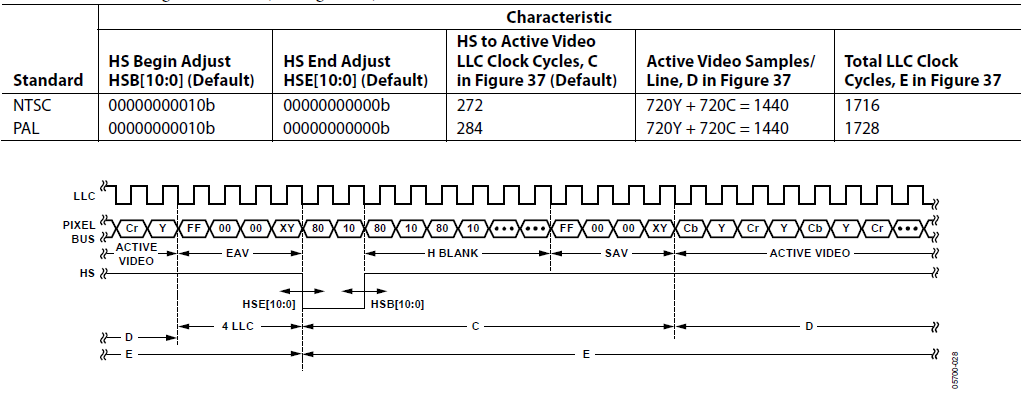
Figure 2: Parameters and timing diagram of the parallel output of ADV7180 codec
The data transferred from the FPGA to the PC is stored in a vector A, of 1048,576 elements (results from 2 ^ 20 with a 20-bit address), then this vector is used for the conversion from YCbCr to RGB. Plotting of A vector is shown in Figure 3.
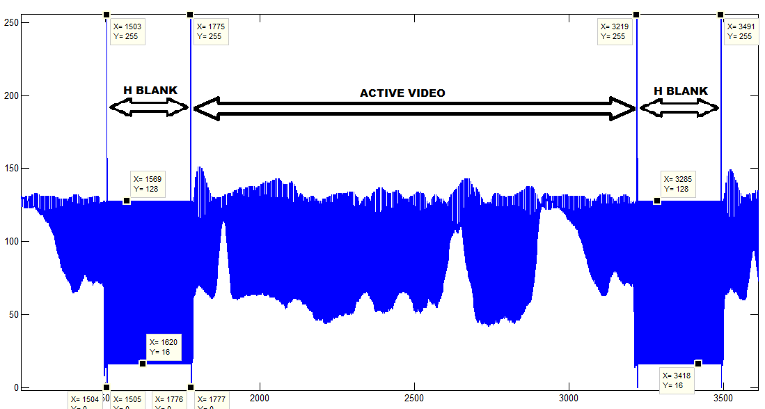
Figure 3: Part of the data received and plotted with Matlab
Figure 2 shows the basic diagram of system states, so the master (PIC32) send a command to read or write the SRAM. Once the reading or writing is finished, the command reading (writing or reading) sent by the master is performed again.
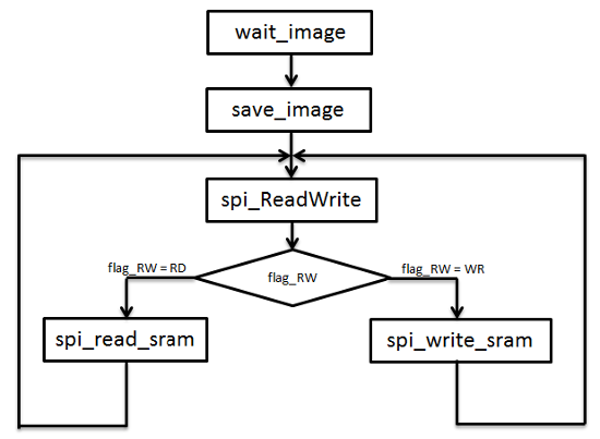
Figure 4: Basic diagram of the states of the system
Figure 4 shows the previous scheme in detailed, so the simplified ASM letter of the finite state machine implemented in the FPGA is shown. This state machine controls the SRAM and SPI modules to perform a correct recording of the image in the SRAM and a correct transmission of data from the SRAM memory to the PIC32.
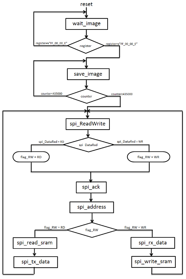
Figure 5: ASM chart of the state machine implemented in the FPGA
As Figure 5 shows, the state machine has 6 main states and are detailed below:
- wait_image: waiting for the starting pattern of the image in order to have a writing of the whole image in the SRAM.
- save_image: writing the image in the SRAM.
- spi_ReadWrite: receives the command (to read or write in the SRAM) by SPI.
- spi_address: receives the address of the SRAM (where to read or written) by SPI.
- spi_read_sram / spi_write_sram: reads or records the value received by SPI at the previously specified address. In the reading of the SRAM by SPI, first there is the state spi_read_sram and then spi_tx_data since first the reading of the SRAM must be done and then the transmission by SPI of the data to the pic32. In the case of writing to the SRAM, the spi_rx_data state is before the spi_write_sram state, since you need to know the value of the data before it is written into memory.
- spi_tx_data / spi_rx_data: transmits or receives by SPI the data that will be read or written in the SRAM.
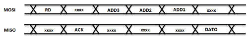
Figure 6: Time diagram for reading the SRAM by SPI
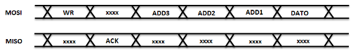
Figure 7: Time diagram for writing the SRAM by SPI
The timing diagram used in the transmission of data by SPI is shown in Figures 4 and 5. So, first the reading command (RD) or writing (WR) of the SRAM is sent, then the PIC32 is obtain a response with the ACK, next the address is sent in three bytes (ADD3, ADD2 and ADD1) since the complete address covers a size of 19 bits and does not reach with a single byte, and finally the data (DATA) is sent or received. is going to write or read in the SRAM. The 6 stages described above were performed consecutively for reading or writing in the SRAM according to master request (in this case the PIC32 is the master).
To perform the test of sending data from the FPGA to the PIC32 microcontroller and show the image on the PC, the PIC32 - PC communication was implemented by UART. Also, the Matlab software was used.
Figure 8: Image captured
As Figure 8 shows, the desired image is obtained. With the previous result, the correct operation of the transmission by SPI is verified. Furthermore, the whole system was implemented in VHDL language and using the Spartan-3 board from Xilinx.